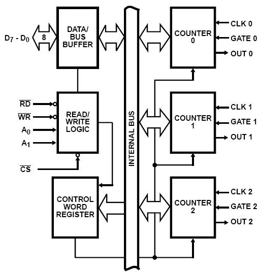
Block diagram of 8253
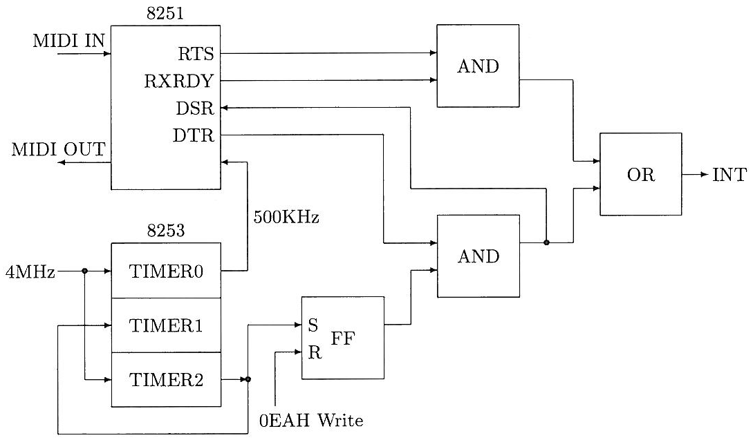
MSXMIDI
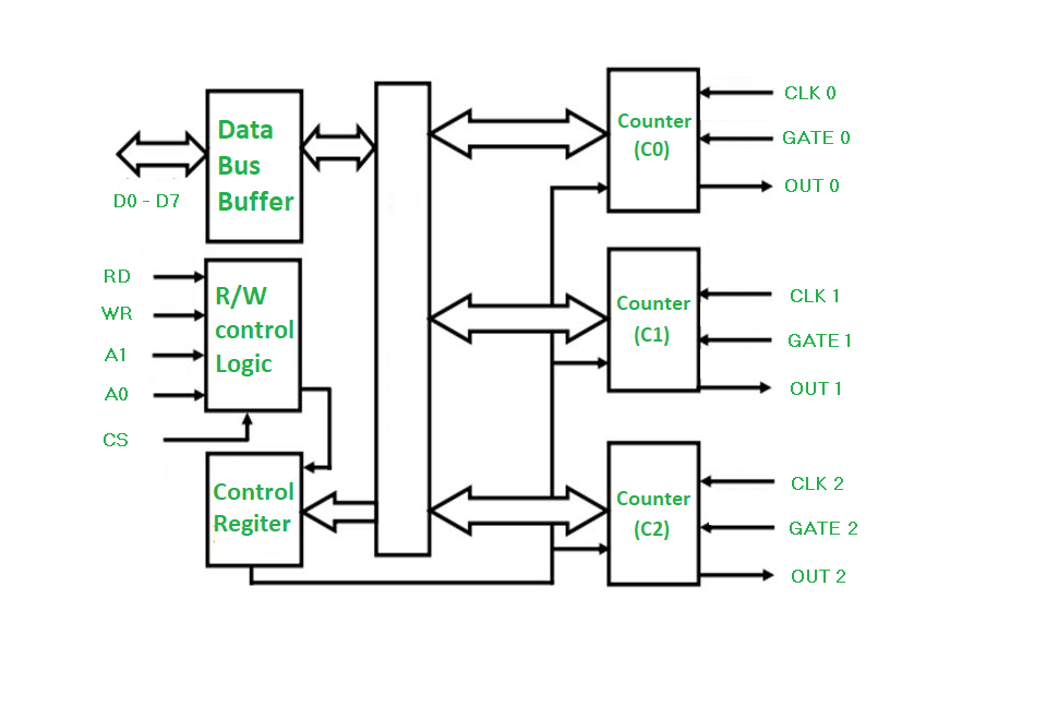
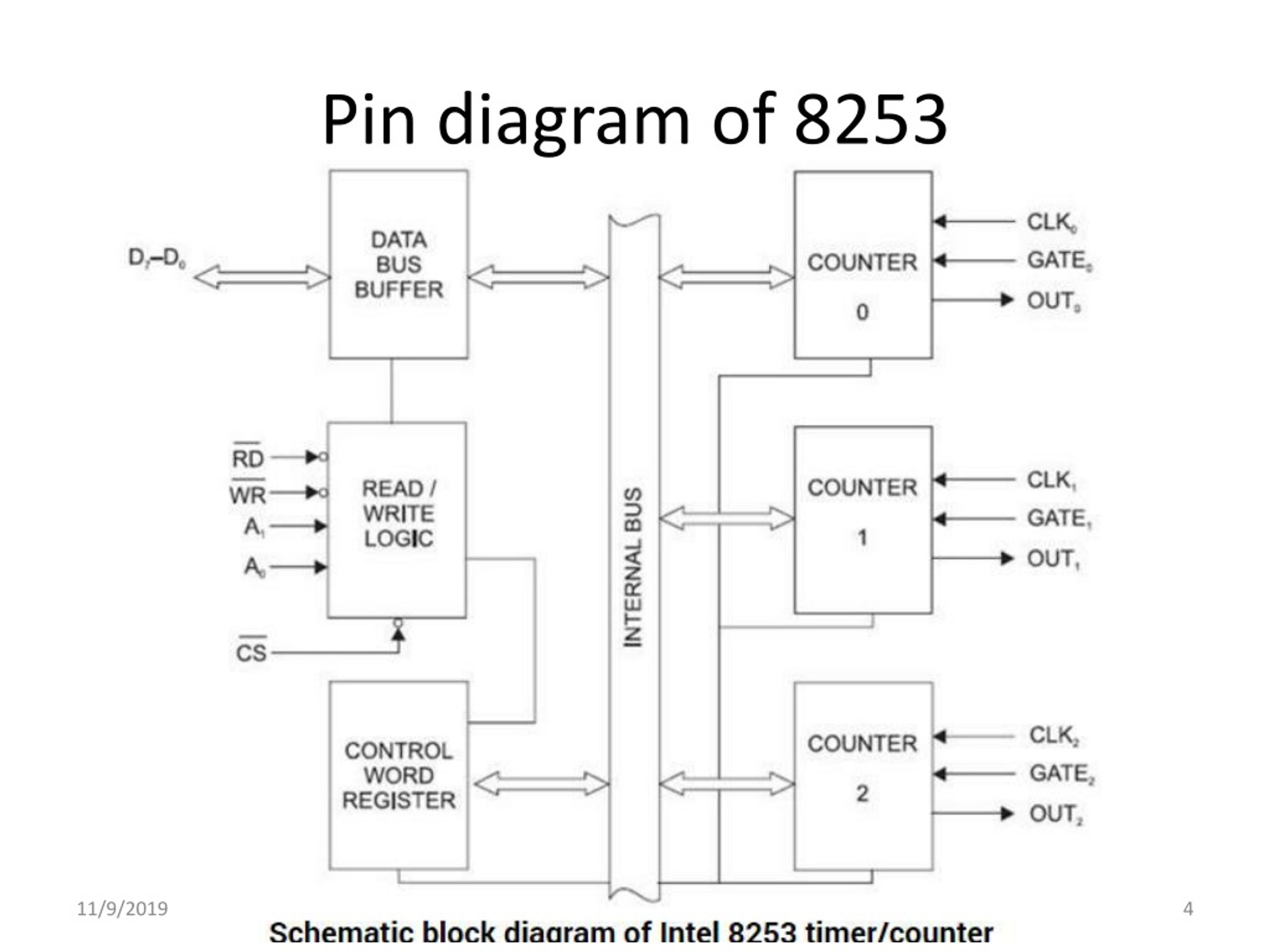
Block diagram of Intel 8253 The timer has three counters, numbered 0 to 2. [7] Each channel can be programmed to operate in one of six modes. Once programmed, the channels operate independently. [1] Each counter has two input pins - "CLK" ( clock input) and "GATE" - and one pin, "OUT", for data output.

Write a control word for counter 1 of 8253 / 8254, Electrical Engineering
The Intel 8254 is a counter/timer device designed to solve the common timing control problems in microcom- puter system design. It provides three independent 16-bit counters, each capable of handling clock inputs up to 10 MHz. All modes are software programmable. The 8254 is a superset of the 8253.
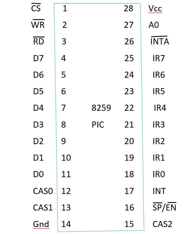
Introduction to 8259 (8259 microprocessor) Interrupt Handling Bcis
Intel 8254 is a programmable interval timer designed by intel is a programmable external timer device built with an aim to resolve the time control issues that occur in between various processes occurring within the microprocessor. In order to communicate with the processor, it has a total of 8 data lines.
CSE TUBE CS2252 / CS42 / 10144 CS403 / 80250010 / EC1257
In this video, i have explained Programmable Interval Timer 8254/8253 by following outlines:0. Programmable Interval Timer 8254/82531. Basics of Programmable.

8253/8254 Programmable Interval Timer Block diagram Complete
It covers complete description of 8253 IC ( PIT) viz. pin diagram, block diagram and working modes.

Fig. C.4 The control word and bit definitions of 8253 (PIT) Download
8254 is a device designed to solve the timing control problems in a microprocessor. It has 3 independent counters, each capable of handling clock inputs up to 10 MHz, and size of each counter is 16 bit. It operates in +5V regulated power supply and has 24 pin signals. All modes are software programmable.
PPT Lecture 3 PowerPoint Presentation, free download ID4572821
File:Intel 8253 block diagram.svg. Size of this PNG preview of this SVG file: 590 × 440 pixels. Other resolutions: 320 × 239 pixels | 640 × 477 pixels | 1,024 × 764 pixels | 1,280 × 955 pixels | 2,560 × 1,909 pixels. Original file (SVG file, nominally 590 × 440 pixels, file size: 29 KB) This is a file from the Wikimedia Commons.
Microprocessor 8254 programmable interval timer
8253/54 Programmable Interval Timer explained with following Timestamps:0:00 - 8253/54 Programmable Interval Timer1:49 - Features of Programmable Interval Ti.

Block Diagram of 8253 8254 YouTube
A "low" on this input enables the 8253. No reading or writing will occur unless the device is selected. The CS input has no effect upon the actual operation of the counters. 8253 BLOCK DIAGRAM CS RD WR Ai A0 0 1 0 0 0 Load Counter No. 0 0 1 0 0 1 Load Counter No. 1 0 1 0 1 0 Load Counter No. 2 0 1 0 1 1 Write Mode Word 0 0 1 0 0 Read.
Pin On Diagrams Gambaran
The block diagram of 8253 Interfacing 8253 with 8085 Now let us see how to interface this 8253 timer chip with the Intel 8085 microprocessor. From the following picture, we can see that the data bus D 7-0 of 8085 is connected to the data pins D 7 to D 0 of 8253.
CSE TUBE CS2252 / CS42 / 10144 CS403 / 80250010 / EC1257
The Intel 8253 and 8254 are Programmable Interval Timers (PTIs) designed for microprocessors to perform timing and counting functions using three 16-bit registers. Each counter has 2 input pins, i.e. Clock & Gate, and 1 pin for "OUT" output. To operate a counter, a 16-bit count is loaded in its register.
8253
Micro44: 8253/8254 Programmable Interval Timer | 8253 Block Diagram | 8254 Block Diagram - YouTube Microprocessor Handwritten Notes (AKTU Syllabus): https://imojo.in/22m2qfi Download.
PPT Programmable interval timer/counter (IC 8253) PowerPoint
It has three basic functions − Programming the modes of 8253/54. Loading the count registers. Reading the count values. Read/Write Logic It includes 5 signals, i.e. RD, WR, CS, and the address lines A0 & A1. In the peripheral I/O mode, the RD and WR signals are connected to IOR and IOW, respectively.

Micro44 8253/8254 Programmable Interval Timer 8253 Block Diagram
The 82C54 is pin compatible with the HMOS 8254, and is a superset of the 8253. Six programmable timer modes allow the 82C54 / 8253 to be used as an event counter, elapsed time indicator, programmable one-shot, and in many other applications. 4.4.1 Block diagram. The timer has three independent, programmable counters and they are all identical. The

8253/8254 Programmable Interval Timer Block Diagram and Pin
The 82C54 is pin compatible with the HMOS 8254, and is a superset of the 8253. Six programmable timer modes allow the 82C54 / 8253 to be used as an event counter, elapsed time indicator, programmable one-shot, and in many other applications. Block diagram
8253 Programmable Timer
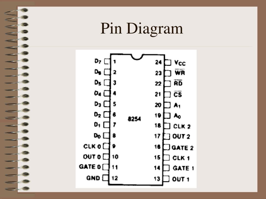
The pin diagram, block diagram of 8253, interfacing with 8085 microprocessor and operation of each mode have been explained in this section. Pin Diagram of 8253 The 8253 timer is a 24-pin IC and operates at +5 V dc. It consists of three independent programmable 16-bit counters: Counter 0, Counter 1, and Counter 2.
